
Showcase Made with Synth
24 V to 3.3 V buck converter
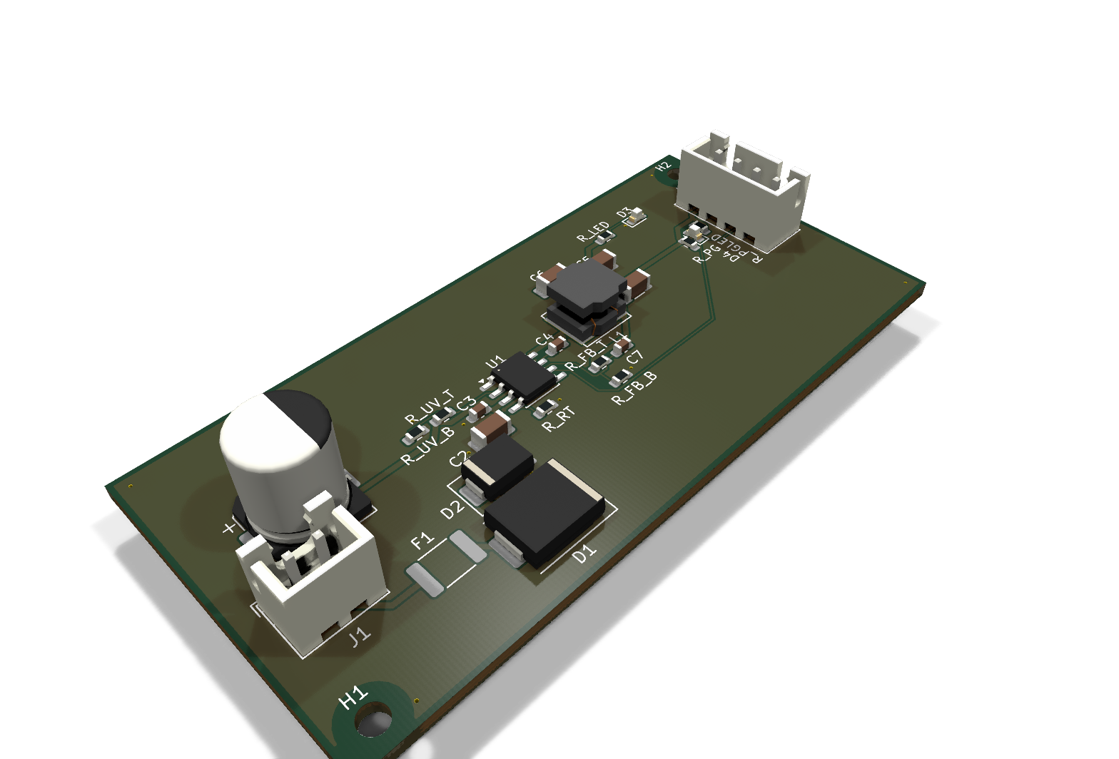
24 V in. 3.3 V out. Power-good on the header.
Overall size 70.99 × 33.99 mm · Layers 4 · Nets routed 13 of 13 · KiCad DRC 0 errors, 0 warnings
Engineering draft. Not fabricated. Not tested on hardware. Reviewed by Steve Munene.
The brief
What the AI was asked, and with what.
Intended use: a bench or prototype 24 V rail, with a 1 A load and a short input cable. It is not for automotive, industrial or mains-derived 24 V systems, and it is not a general-purpose module: the input has a PTC, a reverse-block Schottky and a TVS, but the board is not surge-tested and no thermal or loop-stability result exists. 24 V nominal (+10%, 26.4 V maximum) comes in on J1, and 3.3 V at 1 A comes out on J2, with power-good on pin 3. The converter is a TI LMR38010 at 800 kHz, with a 6.8 µH inductor and three 22 µF output capacitors. Feedback is taken from the output node, never from the switch node; the published negative twin takes it from SW, and the rule rejects it. Power-good is open drain with a 100 kΩ pull-up, and a green LED lights while PG is low. A second green LED shows the 3.3 V rail. A UVLO divider starts the converter at about 18.4 V and stops it at about 16.2 V.
The brief in one sentence
A 24 V to 3.3 V, 1 A buck converter with a PTC, reverse-block Schottky and TVS on the input, power-good and thermal vias in the regulator pad, where every claim must be true and measured.
There is no single prompt: the board came from an agent session plus hand review. The prompt below is a cleaned, self-contained version of that brief, with our local setup removed, so you can run it yourself. It is not the exact text we ran, and it describes the published board (the merged absmach/synth#110). A different run will not give an identical board.
Read the prompt you can run
# Prompt: 24 V to 3.3 V buck converter

A self-contained prompt for an AI agent that can read and write files and run shell commands. It builds the board shown on this page with Synth. The board, its parts and the design decisions with their reasons are in the prompt. Synth's own documentation covers the exact command options and the `.synth` syntax.

This is a cleaned version of the brief we gave the agent: same board and decisions, with our local setup removed. It is not the exact text we ran, and a different run will not produce an identical board.

## You need

- Synth (the `synth` command, which compiles a `.synth` file to a KiCad project), with its part registry.
- KiCad 10 (`kicad-cli`) and FreeRouting 2.4.1 with Java, which Synth's export uses to route.
- An AI model that can use Synth through its command line or its MCP server, and read manufacturer datasheets from the web.

## The prompt

You are designing a real 24 V to 3.3 V step-down converter board with Synth, which compiles a `.synth` source file into a deterministic KiCad project. The board will be published, so every claim you make must be true and measured. Do not call the board clean, proven or manufacturable.

Rules: edit only the `.synth` source and its placement layout file, never the generated KiCad files. The placement layout is in board millimetres and the schematic layout is in sheet millimetres; never mix them. If a part is missing from the registry, author a Tier-2 part from its datasheet; never guess pin numbers.

### The board

24 V nominal input, up to 26.4 V (+10%), and 3.3 V at 1 A output. Use four copper layers with GND pours on all of them and a hand-pinned placement. Say in the README what the board is not: not surge-tested, not thermally characterised, not fabricated.

Input chain: J1 (JST XH, 2-pin: pin 1 +24 V, pin 2 GND) -> F1 resettable PTC (Ihold 1.1 A, Vmax 33 V) -> D1 SS36 Schottky in series (reverse-polarity block) -> VIN node.

VIN node: D2 SMBJ30A TVS (30 V standoff, 48.4 V clamp at 12.4 A), C1 47 uF 50 V electrolytic, C2 10 uF 50 V X7R 1206, C3 220 nF 50 V X7R 0603 at the regulator's VIN pin, U1 VIN, and the top of the UVLO divider.

Regulator: TI LMR38010SDDAR, 4.2 to 80 V operating, 85 V absolute maximum, 1 A, internal compensation, exposed pad (pin 9) on GND, open-drain PG. R_RT 33k from RT/SYNC to GND sets 800 kHz; the pin must not float. C4 100 nF between BOOT and SW.

UVLO: R_UV_T 1.37M from VIN to EN, R_UV_B 100k from EN to GND. Nominal start 18.4 V, stop 16.2 V from the datasheet's typical thresholds; state the min/max spread and say the extremes are not a guaranteed hysteresis.

Output: L1 6.8 uH (Bourns SRN6045TA) from SW to the output node, then C5, C6 and C9, three 22 uF 25 V X7R 1206 capacitors. Feedback R_FB_T 100k from the output node (the far side of L1, never SW) to FB, R_FB_B 43.2k from FB to GND, C7 56 pF across R_FB_T. Vout is 3.315 V typical.

Power-good: R_PG 100k from PG to +3V3, and the PG net goes to J2 pin 3. D4 is a green LED with R_PGLED 470 ohm from +3V3 to PG, so it is lit while PG is low (start-up or fault) and dark while power is good. D3 is a green power LED with R_LED 470 ohm from +3V3.

Connector: J2 is a JST XH 4-pin: pin 1 +3V3, pin 2 GND, pin 3 power-good, pin 4 GND. Put J1 on the left edge and J2 on the right edge with hard placement hints.

Mechanical: H1 and H2 are M2.5 non-plated mounting holes in opposite corners.

Placement: pin every part in the sidecar. Put the input chain below U1 so VIN does not cross the EN divider, C3 and C2 close to the VIN pad, C5, C6 and C9 in a short column beside L1's output pad, and the feedback parts close to FB. Add six 0.3 mm GND vias in U1's exposed pad as sidecar `[[vias]]`, and declare `requires via_in_pad` with manufacturer `jlc-filled-via`.

### Checks

- `synth validate` must pass with no error. Warnings are acceptable only if you list them and their reason.
- Build a negative twin with R_FB_T and C7 taken from SW instead of the output node. It must fail validation with E-SYNTH-POWER-011. Publish it and say what it proves.
- Export with FreeRouting and run `kicad-cli pcb drc --severity-all --refill-zones` on the delivered board: target 0 errors, 0 warnings, 0 unconnected items.
- Run `kicad-cli sch erc --severity-all`: target 0 violations.
- Check that every net is connected, the GND pour is stored filled, and the via-in-pad list is exactly the six thermal vias.

### What to write down

Report the measured size, layer count, net count, segment and via count, copper length, DRC and ERC results, and the router and its version. List what is not verified: no expert signal-integrity, power-integrity or RF review; no thermal measurement or junction-temperature estimate; no loop-stability or load-transient result; no input or output ripple measurement; no surge test and no IEC 61000-4-5 claim; no DC-bias data for the ceramics; no LCSC numbers or MPN for the generic passives; and no fabrication. State that the six filled vias in the pad are not confirmed with a fab. Do not present Synth's release gate as a manufacturing sign-off.
Model and tools
- AI model
- Claude Sonnet 5.5 (claude-sonnet-5-5), run in Claude Code
- Synth MCP
- placement review and validation during the design; the placement review was not rerun on the final hand-pinned board
- Manufacturer datasheets
- TI, Vishay, Bourns, JST, Lite-On and Honor Elec datasheets, read from the web and cited in the qualification matrix
- Command line
- synth validate, synth registry qualify and synth export-kicad, then kicad-cli DRC, ERC, Gerber, drill, 3D render and GLB/STEP export. These did not go through MCP.
The source
The board is a plain-text file. Synth compiles it to a KiCad project.
The whole file, buck.synth, 161 lines. Scroll the box, or copy the file.
// SYN-67: 24 V in, 3.3 V out buck (TI LMR38010) with input parts (PTC, reverse-block diode, TVS).
// Intended for 24 V +10% in and 1 A out.
//
// Input chain: J1 -> F1 (PTC) -> D1 (Schottky reverse block) -> VIN node.
// VIN node: D2 (TVS), C1 (bulk), C2 (10 uF), C3 (220 nF, on the VIN pin), U1 VIN, R_UV_T.
// LMR38010: 4.2-80 V input (85 V absolute maximum), 1 A, 800 kHz set by RT, internal compensation, exposed thermal pad, open-drain PG.
// The SMBJ30A (VBR 33.3-36.8 V, clamp 48.4 V) clamps surges at the VIN node; its clamp is below U1's 85 V absolute maximum.
// Feedback divider is tapped from the output node (L1.p2), never from SW.
board "buck" {
  layers 4
  manufacturer "jlc-filled-via"
  revision "A"

  netclass "PWR" {
    trace_width 0.5mm
    clearance 0.2mm
  }

  power "VIN" 24v
  power "+3V3" 3.3v

  group "INPUT PROTECTION" color "#c2410c" {
    component J1: connector "jst_b2b_xh_a_2pin" value "24V_IN" { placement_hint { region: left_edge edge: left priority: hard } }
    component F1: fuse "mf_msmf110_33x" value "1.1A_PTC"
    component D1: diode "ss36" value "SS36"
    component D2: diode "smbj30a" value "SMBJ30A"
    notes "" {
      "J1 pin 1 is +24 V, pin 2 is GND."
      "F1 resettable PTC: Ihold 1.1 A, Vmax 33 V."
      "D1 Schottky in series blocks reverse polarity."
      "D2 TVS (30 V standoff) sits after D1, directly on the VIN node. Its 48.4 V clamp is below U1's 85 V absolute maximum, so U1 stays within its rating under a surge the TVS can absorb."
    }
  }

  group "INPUT FILTER" color "#7c3aed" {
    component C1: capacitor "c_electrolytic_smd_8x10" value "47uF" voltage "50V"
    component C2: capacitor "c_generic_1206" value "10uF" dielectric "X7R" voltage "50V"
    component C3: capacitor "c_generic_0603" value "220nF" dielectric "X7R" voltage "50V"
    notes "" {
      "C1 bulk, C2 ceramic, C3 high-frequency next to the VIN pin (LMR38010 section 9.2.2.6: at least 4.7 uF + 100 to 220 nF)."
      "50 V parts for a 24 V rail; DC-bias derating of C2 is not known."
    }
  }

  group "UVLO" color "#0a7d4a" {
    component R_UV_T: resistor "r_generic_0603" value "1.37M" tolerance "1%"
    component R_UV_B: resistor "r_generic_0603" value "100k" tolerance "1%"
    notes "" {
      "EN divider from VIN. LMR38010 VEN-H 1.25 V typical (1.1 to 1.4), VEN-L 1.10 V typical: start 18.4 V (16.2 to 20.6 V), stop 16.2 V."
      "EN stays under 2 V at a 28 V input (EN absolute maximum is VIN + 0.3 V)."
    }
  }

  group "BUCK" color "#0072b2" {
    component U1: regulator "lmr38010"
    component C4: capacitor "c_generic_0603" value "100nF" dielectric "X7R" voltage "16V"
    component R_RT: resistor "r_generic_0603" value "33k" tolerance "1%"
    component L1: inductor "l_bourns_srn6045ta_6r8m" value "6.8uH"
    component C5: capacitor "c_generic_1206" value "22uF" dielectric "X7R" voltage "25V"
    component C6: capacitor "c_generic_1206" value "22uF" dielectric "X7R" voltage "25V"
    component C9: capacitor "c_generic_1206" value "22uF" dielectric "X7R" voltage "25V"
    notes "" {
      "LMR38010SDDAR: internal compensation, exposed pad (pin 9) on GND, open-drain PG, PFM with spread spectrum."
      "R_RT 33k from RT/SYNC to GND sets 800 kHz (RT table under datasheet Figure 8-4); the pin must not float."
      "C4 100 nF boot capacitor between BOOT and SW."
      "L1 6.8 uH at 800 kHz gives about 0.5 A ripple at 26.4 V in (datasheet Eq 10 K about 0.5), above the 1.03 uH minimum of Eq 11 (0.25 x 3.3 V / 800 kHz); 3x 22 uF is unverified: Table 9-1 has no 3.3 V row."
      "The exposed pad (pin 9) is soldered to the F.Cu GND pour. There are no vias in the pad:"
      "the board's fabrication floor is a 0.3 mm drill and the KiCad thermal-via footprint ships 0.2 mm."
    }
  }

  group "FEEDBACK" color "#b45309" {
    component R_FB_T: resistor "r_generic_0603" value "100k" tolerance "1%"
    component R_FB_B: resistor "r_generic_0603" value "43.2k" tolerance "1%"
    component C7: capacitor "c_generic_0603" value "56pF" dielectric "C0G" voltage "50V"
    notes "" {
      "Vout = 1.0 V x (1 + 100k / 43.2k) = 3.31 V."
      "Divider taps the output node on the far side of L1, not SW."
      "C7 56 pF feed-forward across the upper resistor (datasheet Eq 9 gives about 60 pF)."
    }
  }

  group "POWER GOOD" color "#4d7c0f" {
    component R_PG: resistor "r_generic_0603" value "100k"
    component D4: led "ltst_c190kgkt" value "PG FAULT"
    component R_PGLED: resistor "r_generic_0603" value "470"
    notes "" {
      "PG is open drain and pulled up to +3V3 through 100k (datasheet 8.3.5: pull up through a resistor; PG tolerates 20 V)."
      "PG goes low during start-up and on a fault, so J2 pin 3 reads valid only after the 4 ms start-up delay."
      "D4 green fault LED from +3V3 through R_PGLED to PG: it is lit while PG is low, dark while power is good."
      "About 2.5 mA when lit (470 R, Vf about 2.1 V); U1's PG pull-down is about 92 ohm RDSON, so PG stays near 0.4 V."
    }
  }

  group "OUTPUT" color "#be123c" {
    component J2: connector "jst_b4b_xh_a_4pin" value "3V3_OUT" { placement_hint { region: right_edge edge: right priority: hard } }
    component D3: led "ltst_c190kgkt" value "PWR"
    component R_LED: resistor "r_generic_0603" value "470"
    notes "" {
      "J2 pin 1 is +3.3 V, pin 2 GND, pin 3 power-good (3.3 V logic, 100k pull-up), pin 4 GND."
      "D3 green power LED from the 3.3 V rail."
    }
  }

  group "MECHANICAL" color "#475569" {
    component H1: mounting_hole "mounting_hole_m2_5" value "M2.5"
    component H2: mounting_hole "mounting_hole_m2_5" value "M2.5"
    notes "" {
      "Two M2.5 non-plated holes in opposite corners; the board is fixed down through them."
    }
  }

  net "VIN_RAW" class "PWR" {
    J1.p1, F1.p1
  }

  net "VIN_FUSED" class "PWR" {
    F1.p2, D1.anode
  }

  net "VIN" class "PWR" {
    D1.cathode, D2.cathode,
    C1.p1, C2.p1, C3.p1,
    U1.vin, R_UV_T.p1
  }

  net "GND" class "PWR" {
    J1.p2, D2.anode,
    C1.p2, C2.p2, C3.p2,
    U1.gnd, U1.pad, R_UV_B.p2,
    C5.p2, C6.p2, C9.p2, R_FB_B.p2, R_RT.p2,
    J2.p2, J2.p4, D3.cathode
  }

  net "SW" class "PWR" {
    U1.sw, L1.p1, C4.p2
  }

  net "+3V3" class "PWR" {
    L1.p2, C5.p1, C6.p1, C9.p1,
    R_FB_T.p1, J2.p1, R_LED.p1, R_PG.p2, R_PGLED.p1
  }

  net "PG" {
    U1.pg, R_PG.p1, J2.p3, D4.cathode
  }

  connect U1.rt_sync -> R_RT.p1 as "RT"
  connect U1.boot -> C4.p1 as "BOOT"
  connect U1.en -> R_UV_T.p2 as "EN"
  connect U1.en -> R_UV_B.p1 as "EN"
  connect U1.fb -> R_FB_T.p2 as "FB"
  connect U1.fb -> R_FB_B.p1 as "FB"
  connect U1.fb -> C7.p1 as "FB"
  connect C7.p2 -> R_FB_T.p1 as "+3V3"
  connect R_LED.p2 -> D3.anode as "LED_PWR"
  connect R_PGLED.p2 -> D4.anode as "LED_PG"

  requires via_in_pad

}
The board
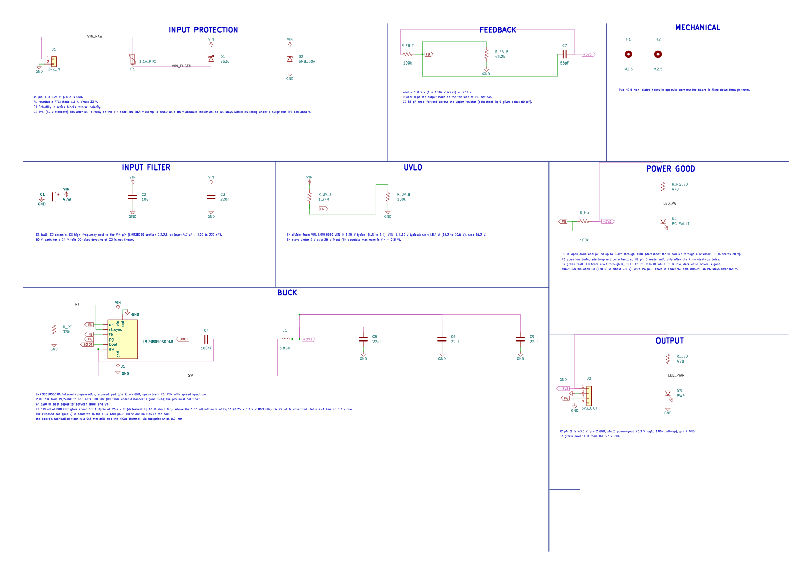
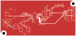
Schematic, every copper layer and the parts, from the same files.
Parts
| Reference | Part | Role |
|---|---|---|
| U1 | TI LMR38010SDDAR | 24 V to 3.3 V synchronous buck, 1 A, 800 kHz, exposed pad on GND |
| L1 | Bourns SRN6045TA | 6.8 µH shielded inductor from SW to the output node |
| D1 | Vishay SS36 | 3 A 60 V Schottky in series, reverse-polarity block |
| D2 | Vishay SMBJ30A | 600 W transient suppressor on the VIN node, 48.4 V clamp |
| F1 | Bourns MF-MSMF110/33X | Resettable PTC, 1.1 A hold, 33 V maximum |
| C1 | Honor Elec 47 µF | Input bulk electrolytic, 50 V |
| C2 C3 | 10 µF and 220 nF | 50 V X7R ceramics at the VIN pin |
| C5 C6 C9 | 3 × 22 µF | 25 V X7R output ceramics |
| R_UV_T R_UV_B | 1.37 MΩ and 100 kΩ | UVLO divider: 18.4 V start, 16.2 V stop, typical |
| R_FB_T R_FB_B C7 | 100 kΩ, 43.2 kΩ and 56 pF | Feedback divider from the output node, 3.315 V typical |
| R_RT | 33 kΩ | Sets the switching frequency to 800 kHz |
| R_PG | 100 kΩ | Open-drain power-good pull-up to 3.3 V |
| D3 D4 | Lite-On LTST-C190KGKT | Green power LED and green PG-fault LED, 470 Ω each; D4 is lit while PG is low |
| J1 J2 | JST XH | 2-pin 24 V input and 4-pin output: 3.3 V, GND, power-good, GND |
| H1 H2 | M2.5 mounting holes | Non-plated holes in opposite corners |
Checks
What was measured, and what was not.
Measured
- Routing
- 13 nets connected, 0 open; 97 segments, 21 vias, 200.08 mm of copper. Every segment is on F.Cu and all 21 vias are GND, six of them in U1's pad. Record: reports/buck.routing.json
- KiCad design-rule check
- 0 errors, 0 warnings, 0 unconnected items, from `kicad-cli pcb drc --severity-all --refill-zones` with the project's custom rules (copper to a board edge 0.3 mm, to a hole or an NPTH hole 0.2 mm, from the JLCPCB profile). The ground pour is stored filled. Report: reports/buck.kicad-drc.json
- Schematic ERC
- 0 violations, run with the KiCad libraries installed. Report: reports/buck.kicad-erc.json
- Release gate
- Passed: release_ready and fabrication_ready are true in Synth's records. That means Synth's own checks passed (routed, 0 open nets, KiCad DRC clean). It is not a manufacturing sign-off: nothing was fabricated or tested, and the fabrication note below applies. Records: reports/release.json, reports/release-fab.json, reports/buck.routing.json
- Fabrication note
- Six vias in U1's exposed pad are via-in-pad. The board declares jlc-filled-via and requires filled and capped vias. Not confirmed with a fab.
- Manufacturing gate disagreement
- `synth check --fab` does not agree: that stage routes with KiCadRoutingTools, whose copper leaves 11 signal vias without a ground return via within 0.64 mm, so it fails manufacturing. The published board was routed with FreeRouting and has no W-SYNTH-DRC-016 finding. The qualification matrix keeps expect_fab = fail for that reason.
- Part reviews
- Eight of the board's nine registry parts are covered by `synth registry qualify`, and all eight qualify (record: reports/registry-qualify.txt). LMR38010 and LTST-C190KGKT were reviewed on 2026-10-29, the rest of the reviewed parts on 2026-10-28. The generic passives and the mounting holes have no MPN or review record.
- Published files
- Board, schematic, source, layout and report files are copied from absmach/synth#110 as merged, revision f1d3947 (qualification/class-b/buck/). The LMR38010 and LTST-C190KGKT reviewer-status paragraphs in QUALIFICATION.md are corrected to match the registry; the same fix is in absmach/synth#404. The 3D model, copper-layer SVGs, schematic SVG and the render are made from that board by KiCad 10.0.7 with the ground pours refilled.
- Synth build
- The routing and release reports were produced on Synth a79570c, the source_revision recorded in reports/buck.routing.json.
Not claimed
- Four copper layers on KiCad's default 1.6 mm stackup, with GND pours on all four. There is no declared stackup and no controlled-impedance net.
- No thermal result. Synth's thermal-relief analysis is unsupported (the relief gap and spoke width are export defaults), U1's exposed pad carries six 0.3 mm vias where TI's datasheet asks for at least a 4 × 3 array of 10 mil vias, and no junction temperature is estimated. The datasheet's RθJA is not valid for design.
- The six vias in U1's pad are via-in-pad. The board declares jlc-filled-via and requires filled and capped vias; no fab has confirmed it.
- Input transient protection is datasheet-only. The SMBJ30A clamps at 48.4 V against the regulator's 85 V absolute maximum, but nothing was surge-tested, no IEC 61000-4-5 rating is claimed, and a sustained overvoltage relies on the PTC and the 50 V capacitors.
- Filtering and loop stability are unverified. TI's datasheet table has no 3.3 V row, the DC-bias derating of C2, C5, C6 and C9 is unknown, and crossover, phase margin and load-transient response were not computed or measured.
- Power-good behaviour is unverified. The connection, pull-up and LED are proven; the 110/112/114 % rising and 90/92/94 % falling thresholds, the 40 µs glitch filter and the 4 ms start-up delay are datasheet numbers that nothing here checks.
- Return-path analysis is a proximity test only. Every layer change is a GND via (all 21 vias are GND), and W-SYNTH-DRC-016 finds none within 0.64 mm, but Synth's capability descriptor still declares return-path analysis unsupported.
- The placement is hand-pinned and not scored. C3 is 0.82 mm and C2 1.46 mm from U1's VIN pad, and C5/C6/C9 are 0.83/2.29/0.70 mm from L1's output pad; R_PG is 22.63 mm from the PG pin and R_FB_B's ground is 11.31 mm from U1 GND, both left as they are.
- Synth's two gates disagree. `synth check --fab` (KiCadRoutingTools) fails manufacturing with 11 signal vias without a ground return via within 0.64 mm, while the published FreeRouting board has none; the matrix row keeps expect_fab = fail.
- Schematic readability is scored, not tidy: 0 overlapping text pairs, 7 texts with a wire through them and 1 wire crossing.
- The comment block in buck.synth still says there are no vias in U1's pad. The placement sidecar adds six, and the exported PCB and connectivity report list them.
- Nothing was fabricated, powered or measured. The generic passives have no MPN and no LCSC number, availability was not checked, and no human reference layout was compared.
- Earlier outlines were 58.0 × 32.6, 70.99 × 31.1 and 60.75 × 31.9 mm. The current 70.99 × 33.99 mm follows the pinned parts and corner holes, and the cause of the final size was not isolated.
Files
Everything on this page, to open in your own tools.
- Design sourceThe .synth file Synth compiles
buck.synth - Negative twinThe feedback-from-SW twin that must fail with E-SYNTH-POWER-011
buck_neg_fb_sw.synth - Placement layoutWhere each part sits on the board, in board millimetres
buck.placement.layout.toml - KiCad PCBRouted board
kicad/buck.kicad_pcb - KiCad schematicGenerated sheet
kicad/buck.kicad_sch - KiCad symbolsGenerated symbol library
kicad/buck.kicad_sym - KiCad projectProject settings
kicad/buck.kicad_pro - KiCad custom rulesCopper to a board edge 0.3 mm, to a hole or NPTH hole 0.2 mm, from the manufacturer profile
kicad/buck.kicad_dru - Bill of materialsReference, value, description
kicad/bom.csv - Symbol library tableThe symbol libraries the generated schematic uses
kicad/sym-lib-table - 3D modelBinary glTF, as shown in the viewer
buck.glb - 3D model (STEP)The board and component models as a STEP assembly, for CAD and enclosure work
buck.step - Route recordSynth's routing run: router, settings, nets, segments, vias
reports/buck.routing.json - Connectivity reportNet-by-net connectivity and the via-in-pad list
reports/buck.connectivity.json - Registry qualificationsynth registry qualify output for the eight parts it covers
reports/registry-qualify.txt - Design-rule checkKiCad 10 DRC report for the routed board
reports/buck.kicad-drc.json - Schematic ERCKiCad 10.0.7 ERC report for the generated schematic
reports/buck.kicad-erc.json - Release gate resultSynth's source and DRC release record
reports/release.json - Manufacturing-package gate resultSynth's record for the Gerber, drill and pick-and-place package
reports/release-fab.json - Qualification matrixWhat was checked, what was not, and what is open. Published as merged; its reproduce section and the Gerber, drill, pick-and-place and pad-gap files live in absmach/synth#110
QUALIFICATION.md - File hashesSHA-256 of every file in this folder except the zip. Regenerated for this folder; the matrix's hash paragraph describes the Synth repository copy
SHA256SUMS - PromptA cleaned version you can run yourself
prompt.md
License
The `.synth` sources, layout files, prompt, KiCad project and images on this page are published in the Synth website repository (github.com/absmach/synth-website), which is licensed under Apache-2.0. The Synth compiler that made them is Apache-2.0 too. The LICENSE file in the zip has the full text, including its disclaimer of warranty.
The KiCad project and the 3D model use footprints and component 3D models from KiCad's official libraries. Those libraries are licensed under CC BY-SA 4.0 with an exception: a design that uses them does not have to be shared under that license (see kicad.org/libraries/license). The zip contains this board only, not the libraries.
This is a description of how the files are published, not legal advice. The board is not fabricated and not tested on hardware.