
Showcase Made with Synth
USB-C dual UART and RS-485 adapter
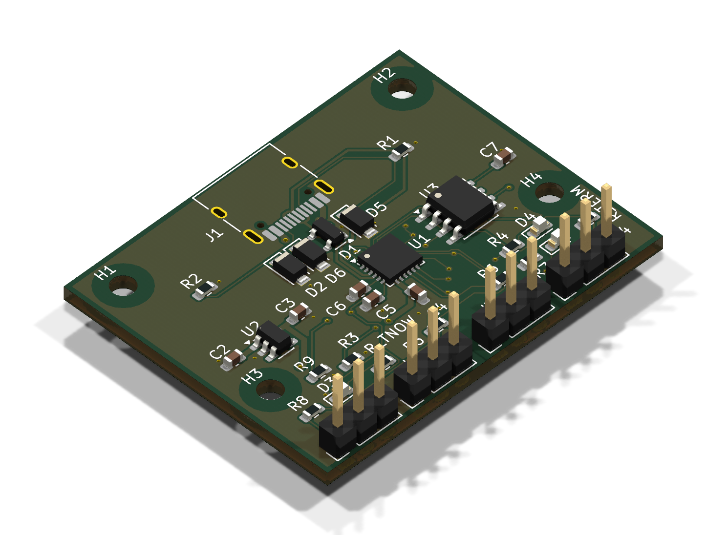
One USB-C cable. Two serial ports.
Overall size 40.99 × 32.23 mm · Layers 2 · Nets routed 26 of 26 · KiCad DRC 0 errors, 0 warnings
Engineering draft. Not fabricated. Not tested on hardware. Reviewed by Steve Munene.
The brief
What the AI was asked, and with what.
Intended use: a bench or lab adapter, with short cables, point-to-point or as the last node on an RS-485 bus. It is not for industrial installs, long cable runs or a node in the middle of a multidrop bus. Port 1 is TTL serial for debugging microcontroller boards: console, flashing, logs. Port 2 is RS-485 for industrial gear such as Modbus sensors, meters and motor drives, and its direction switches by itself from the bridge's DTR0/TNOW0 pin. Power comes from USB, and a jumper picks 3.3 V or 5 V I/O. Protection is on the USB side: a PRTR5V0U2X ESD array on D+ and D-, and PTVS6V0S1UR TVS diodes on VBUS, CC1 and CC2. The RS-485 pair has no external TVS or common-mode choke, and the 120 Ω termination is always in circuit. The two TX LEDs take their current from VIO and sink it into the TX lines, so they are dark while a line idles.
The brief in one sentence
A real USB-C to dual-UART and RS-485 adapter, with USB ESD and TVS protection, where every claim must be true and measured.
There is no single prompt: the board came from a long chat plus agent briefs. The prompt below is a cleaned, self-contained version of that brief, with our local setup removed, so you can run it yourself. It is not the exact text we ran, and it describes the published board (the merged absmach/synth#103). A different run will not give an identical board.
Read the prompt you can run
# Prompt: USB-C dual-UART + RS-485 adapter

A self-contained prompt for an AI agent that can read and write files and run shell commands. It builds the board shown on this page with Synth. The board, its parts and the design decisions with their reasons are in the prompt. Synth's own documentation covers the exact command options and the `.synth` syntax.

This is a cleaned version of the brief we gave the agent: same board and decisions, with our local setup removed. It is not the exact text we ran, and a different run will not produce an identical board.

## You need

- Synth (the `synth` command, which compiles a `.synth` file to a KiCad project), with its part registry.
- KiCad 10 (`kicad-cli`) and FreeRouting 2.4.1 with Java, which Synth's export uses to route.
- An AI model that can use Synth through its command line or its MCP server, and read manufacturer datasheets from the web.

## The prompt

You are designing a real USB-C to dual-UART plus RS-485 adapter board with Synth, which compiles a `.synth` source file into a deterministic KiCad project. The board will be published, so every claim you make must be true and measured. Do not call the board clean, proven or manufacturable.

Rules: edit only the `.synth` source and its placement layout file, never the generated KiCad files. The placement layout is in board millimetres and the schematic layout is in sheet millimetres; never mix them. If a part is missing from the registry, author a Tier-2 part from its datasheet; never guess pin numbers.

### The board

One USB-C cable gives a computer two serial ports.

Intended use: a bench or lab adapter, with short cables, point-to-point or as the last node on an RS-485 bus. It is not for industrial installs, long cable runs or a node in the middle of a multidrop bus: A and B get no surge protection beyond the transceiver's built-in ESD, and the 120 Ω termination is always connected. Say so in the README.

- **Port 1: TTL serial** for debugging microcontroller boards. It comes out on two 3-pin headers: J2 = GND, TXD1, RXD1 (pin 1 is GND), and J3 = DTR1, RTS1, CTS1. Put 1 kΩ in series with RXD1 and with CTS1.
- **Port 2: RS-485** for industrial gear. A 3-pin header J4 = A, B, GND. Put a 120 Ω 1 % resistor across A and B. Its direction switches by itself, from the CH342F's DTR0/TNOW0 pin, with no software control. Put a 4.7 kΩ 1 % resistor from TNOW0 to GND to select the bridge's automatic half-duplex direction mode.
- **Power** comes from USB. A 3-pin jumper J_VIO picks the serial I/O voltage: pin 1 = +3V3, pin 2 = VIO, pin 3 = VBUS. Jumper 1-2 gives 3.3 V, jumper 2-3 gives 5 V. With no jumper, VIO is unpowered; state in the README what the bridge does then, from its datasheet. Think through what a forgotten jumper does to the rest of the board, and say it in the README.

### Parts

- WCH CH342F, dual USB-UART bridge, QFN-24 4 x 4 mm, 0.5 mm pitch, exposed pad to GND. Per its datasheet, its VIO pin sets the I/O voltage of both UARTs.
- TI THVD1450D, 3 to 5.5 V RS-485 transceiver. DI comes from TXD0, RO goes to RXD0, and DE and /RE are tied together and driven by the CH342F's DTR0/TNOW0 pin. Power it from VIO with 100 nF.
- Nexperia PRTR5V0U2X, ESD array on the USB D+/D- pair (VCC pin on VBUS).
- Nexperia PTVS6V0S1UR, 400 W TVS diodes on VBUS, CC1 and CC2, close to the connector.
- TI LP5907-3.3 LDO (SOT-23-5): 2.2 µF in and out, EN tied to VIN. It makes +3V3 for the jumper.
- USB-C receptacle `usb_c_receptacle` (HRO TYPE-C-31-M-12, a stock KiCad footprint), flush with the top board edge and centred along it. Connect all its VBUS pins to VBUS, and its ground and shield pins to GND. CC1 and CC2 each get 5.1 kΩ to GND so a USB-C host supplies 5 V. Both the A-side and B-side D+ and D- pins are tied together (the plug works either way round) and go straight to the bridge with no series resistor. Give them a netclass with 0.242 mm trace width and 0.127 mm clearance. Do not declare a 90 Ω impedance target: on two layers at 1.6 mm it is not reachable, and the pair will not be coupled by the router. Say so in the README.
- LEDs (Lite-On LTST-C190 series, 0603): green on VIO, red on TXD0 and TXD1, each with 470 Ω from VIO into the LED, with the LED's cathode on the TX line. The red LEDs sink their current into the TX pin, so they are dark while a line idles and lit on the low bits.
- Four M2.5 mounting holes H1 to H4, the registry part `mounting_hole_m2_5` as `mounting_hole` components, with hard placement hints: H1 and H2 in the top corners, H3 and H4 on the left and right edges at mid-height. Pin them in the placement layout at x 5.5 and 39.6 mm, y 3.0 mm (H1, H2) and y 21.0 mm (H3, H4). The bottom corners belong to the header row. Each hole must be clear of every other courtyard and keep at least 1.5 mm to Edge.Cuts; Synth adds a 2.2 mm board-feature rim around a hole when it fits the outline. Screw size and standoff height are not chosen.
- Headers J2, J3, J4 and J_VIO are 1 x 3, 2.54 mm pitch, through-hole.
- All resistors and capacitors are 0603. Capacitors are X7R, 16 V.
- 100 nF decoupling on the bridge's VDD5, V3 and VIO pins. Place each within 1 to 2 mm of its pin.
- Pull the CH342F's unused modem inputs (RI0, RI1, DCD0, DCD1, DSR0, DSR1) to VIO through 10 kΩ. Hold CTS0 low through 10 kΩ so UART0 flow control cannot stall. Leave RST open (internal pull-up).

Two decisions already made, with the reason:

1. **No 1.8 V or target-powered mode.** The THVD1450 needs at least 3 V, and it is powered from VIO. So when VIO is powered it is always 3.3 V or 5 V, chosen only by the jumper; with no jumper it is off.
2. **UART0 is not broken out as TTL.** It only drives the RS-485 transceiver. Do not add a TTL header for it.

Board: **2 layers**, manufacturer profile JLCPCB, no declared stackup (the exporter writes the 1.6 mm default). Put the USB-C on the top edge and the four headers (J2, J3, J4, J_VIO) on the bottom edge in one row. Compact placement: aim for roughly 41 x 32.3 mm.

### Tasks, in order

1. **Datasheets.** For each IC, protection part, LED and the connector (not the generic resistors, capacitors and headers), read the manufacturer's own datasheet (not a mirror) and record its revision. If you cannot reach the manufacturer's site, mark that part UNVERIFIED in the README.
2. **Write the design** as one `.synth` file (for example `usb_uart.synth`), with grouped sections (USB-C input, ESD, 3V3 LDO, bridge, VIO select, UART1 TTL, RS-485, LEDs) and a short note in each.
3. **Validate** with `synth validate`. Fix every error. List each remaining warning and what it means.
4. **Schematic.** Export it, render it, and look at the image. Fix power symbols that point the wrong way, overlapping labels, and parts outside their group box.
5. **Placement.** Synth's exporter runs its automatic placer when you export; start from that result, then tune `usb_uart.placement.layout.toml` (board millimetres). Measure each protection part and each decoupling capacitor against its target pad (pad-edge gap), the connector's distance to the board edge, and each mounting hole's distance to Edge.Cuts and to the nearest courtyard.
6. **Route** with `synth export-kicad <file> --out <dir> --router free-routing --krt-allow-via-in-pad`. The flag lets the router put the ground via inside the QFN's exposed pad, which a 0.5 mm pitch part has no room for otherwise. Synth keeps the routed board only if it passes independent validation. Then run `kicad-cli pcb drc --severity-all --refill-zones` on the delivered file. Target: every net connected, 0 DRC errors, 0 unconnected items. The router's result changes with every placement: if nets stay open, or the router leaves a net unrouted, shift the headers by a millimetre or two and route again. Do not accept a USB pair whose two lines differ by more than a few millimetres without saying so.
7. **Check what routing cannot give you.** Report the distance from each decoupling and protection pad to the nearest ground via, and the USB pair's track widths, lengths and skew (per connector contact), and whether it is length-matched or impedance-controlled. Report any via placed inside a pad, and what a fabricator would have to do (fill and cap it) to build it.
8. **README** next to the source: the concept; a bill of materials with part number, manufacturer datasheet URL and revision for every part; the VIO jumper table; the measured numbers (nets, tracks, vias, DRC result, route time); and what is NOT verified: not fabricated, not tested on hardware, any via-in-pad not confirmed with a fabricator, the USB pair not impedance-controlled, any UNVERIFIED part, any open warning. State that R_TERM is always in circuit and that there is no external TVS on A or B.

### Report back

The validate result (counts by code and what remains), the measured distances table, the DRC counts, the routing statistics, every decision you made on the open points and why, and every doubt or thing you could not verify.
Model and tools
- AI model
- Claude Sonnet 5.5 (claude-sonnet-5-5), run in Claude Code
- Synth MCP
- synth_language_reference and synth_validate, once each in the first design round
- Firecrawl MCP
- web search and page scrape to read manufacturer datasheets
- Command line
- synth export, kicad-cli design-rule check, 3D render and GLB export. These did not go through MCP.
The source
The board is a plain-text file. Synth compiles it to a KiCad project.
The whole file, usb_uart.synth, 198 lines. Scroll the box, or copy the file.
// SYN-66 board #66 rework: USB-C to CH342F dual-UART + RS-485 adapter.
//
// UART1 is broken out as TTL at the VIO level (3.3 V or 5 V). UART0 is
// not broken out as TTL: it feeds a THVD1450 RS-485 transceiver, which
// needs at least 3 V, so VIO is never below 3.3 V. VIO (the I/O rail
// for both UARTs and the transceiver) is selected by the J_VIO 3-way
// jumper: +3V3 or VBUS. With no jumper VIO is unpowered and the
// bridge stays in reset.
board "usb_uart" {
  layers 2
  manufacturer "jlcpcb"
  revision "A"

  netclass "USB" {
    trace_width 0.242mm
    clearance 0.127mm
  }

  power "VBUS" 5v
  power "+3V3" 3.3v

  component H1: mounting_hole "mounting_hole_m2_5" { placement_hint { region: top_left priority: hard } }
  component H2: mounting_hole "mounting_hole_m2_5" { placement_hint { region: top_right priority: hard } }
  component H3: mounting_hole "mounting_hole_m2_5" { placement_hint { region: bottom_left priority: hard } }
  component H4: mounting_hole "mounting_hole_m2_5" { placement_hint { region: bottom_right priority: hard } }

  group "USB-C INPUT" color "#c2410c" {
    component J1: connector "usb_c_receptacle" { placement_hint { edge: top priority: hard } }
    component R1: resistor "r_generic_0603" value "5.1k"
    component R2: resistor "r_generic_0603" value "5.1k"
    notes "" {
      "USB 2.0 device port, VBUS 5 V in. D+/D- go straight to U1 (no series R)."
      "CC1/CC2 5.1k Rd to GND so a USB-C host sources 5 V."
    }
  }

  group "ESD" color "#7c3aed" {
    component D1: diode "prtr5v0u2x" value "TVS"
    component D2: diode "ptvs6v0s1ur" value "TVS"
    component D5: diode "ptvs6v0s1ur" value "TVS"
    component D6: diode "ptvs6v0s1ur" value "TVS"
    notes "" {
      "PRTR5V0U2X rail-to-rail clamp on D+/D- (VCC pin on VBUS)."
      "PTVS6V0S1UR on VBUS, CC1 and CC2, close to the connector."
    }
  }

  group "3V3 LDO" color "#0072b2" {
    component U2: regulator "lp5907_3v3" value "LDO"
    component C2: capacitor "c_generic_0603" value "2.2uF" dielectric "X7R" voltage "16V"
    component C3: capacitor "c_generic_0603" value "2.2uF" dielectric "X7R" voltage "16V"
    notes "" {
      "LP5907-3.3: 2.2 uF ceramic in and out."
      "(datasheet minimum is 1 uF)."
      "EN tied to VIN, always on."
    }
  }

  group "CH342F BRIDGE" color "#0a7d4a" {
    component U1: ic "ch342f"
    component C4: capacitor "c_generic_0603" value "100nF" dielectric "X7R" voltage "16V"
    component C5: capacitor "c_generic_0603" value "100nF" dielectric "X7R" voltage "16V"
    component C6: capacitor "c_generic_0603" value "100nF" dielectric "X7R" voltage "16V"
    component R8: resistor "r_generic_0603" value "10k"
    component R9: resistor "r_generic_0603" value "10k"
    notes "" {
      "VDD5 <- VBUS (100nF C4), V3 <- 100nF only (C5), VIO <- VIO net (100nF C6)."
      "VBUS pin <- VBUS net. RST left NC (internal pull-up). EP (pin 25) to GND."
      "R8 10k pulls the unused modem inputs RI0/RI1/DCD0/DCD1/DSR0/DSR1 to VIO (inactive)."
      "R9 10k holds CTS0 low (always clear to send) so UART0 flow control cannot stall."
    }
  }

  group "VIO SELECT" color "#9333ea" {
    component J_VIO: connector "header_1x3" value "VIO_SEL" { placement_hint { edge: bottom priority: hard } }
    notes "" {
      "p1=+3V3, p2=VIO, p3=VBUS."
      "Jumper 1-2: 3.3 V. Jumper 2-3: 5 V."
      "No jumper: VIO off, bridge in reset."
      "Do not wire anything to pin 2."
    }
  }

  group "UART1 TTL" color "#b45309" {
    component J2: connector "header_1x3" value "UART1" { placement_hint { edge: bottom priority: hard } }
    component J3: connector "header_1x3" value "FLOW1" { placement_hint { edge: bottom priority: hard } }
    component R5: resistor "r_generic_0603" value "1k"
    component R6: resistor "r_generic_0603" value "1k"
    notes "" {
      "J2: GND, TXD1, RXD1 (pin 1 is GND)."
      "J3: DTR1, RTS1, CTS1."
      "R5 1k series on RXD1, R6 1k on CTS1."
    }
  }

  group "RS485 UART0" color "#0d9488" {
    component U3: ic "thvd1450d"
    component R_TNOW: resistor "r_generic_0603" value "4.7k" tolerance "1%"
    component C7: capacitor "c_generic_0603" value "100nF" dielectric "X7R" voltage "16V"
    component J4: connector "header_1x3" value "RS485" { placement_hint { edge: bottom priority: hard } }
    component R_TERM: resistor "r_generic_0603" value "120ohm" tolerance "1%"
    notes "" {
      "DI <- TXD0, RO -> RXD0. DE//RE tied together and driven by DTR0/TNOW0."
      "R_TNOW 4.7k to GND on TNOW0 (auto-direction config). VCC <- VIO (100nF C7)."
      "J4: A, B, GND. R_TERM 120 ohm 1% across A/B. UART0 TTL is not broken out."
    }
  }

  group "LEDs" color "#be123c" {
    component D3: led "ltst_c190kgkt" value "VIO"
    component R3: resistor "r_generic_0603" value "470"
    component D4: led "ltst_c190krkt" value "TX0"
    component R4: resistor "r_generic_0603" value "470"
    component D7: led "ltst_c190krkt" value "TX1"
    component R7: resistor "r_generic_0603" value "470"
    notes "" {
      "D3 green LED from VIO (VIO present)."
      "D4/D7 red LEDs from VIO, sunk into TXD0/TXD1: dark while the line idles, lit on the low bits."
      "No ACT# LED: the CH342F QFN24 has no ACT# bond-out."
    }
  }

  net "VBUS" {
    J1.vbus, J1.vbus_b4, J1.vbus_a9, J1.vbus_b9,
    D1.vcc, D2.cathode,
    U2.vin, U2.en, C2.p1,
    U1.vdd5, U1.vbus, C4.p1,
    J_VIO.p3
  }

  net "+3V3" {
    U2.vout, C3.p1, J_VIO.p1
  }

  net "VIO" {
    J_VIO.p2, U1.vio, C6.p1, U3.vcc, C7.p1, R3.p1, R8.p1, R4.p1, R7.p1
  }

  net "GND" {
    J1.gnd, J1.gnd_a12, J1.gnd_b1, J1.gnd_b12, J1.shld,
    R1.p2, R2.p2,
    D1.gnd, D2.anode, D5.anode, D6.anode,
    C2.p2, C3.p2, C4.p2, C5.p2, C6.p2, C7.p2,
    U2.gnd, U1.gnd, U1.ep, U3.gnd,
    J2.p1, J4.p3, R9.p2,
    R_TNOW.p2,
    D3.cathode
  }

  connect J1.cc1 -> R1.p1 as "CC1"
  connect J1.cc1 -> D5.cathode as "CC1"
  connect J1.cc2 -> R2.p1 as "CC2"
  connect J1.cc2 -> D6.cathode as "CC2"

  connect J1.dp -> J1.dp_b6 as "USB_DP" class "USB"
  connect J1.dp -> D1.io1 as "USB_DP"
  connect J1.dp -> U1.ud_plus as "USB_DP"
  connect J1.dn -> J1.dn_b7 as "USB_DN" class "USB"
  connect J1.dn -> D1.io2 as "USB_DN"
  connect J1.dn -> U1.ud_minus as "USB_DN"

  // The USB pair has no impedance target: at 1.6 mm on two layers, 90 ohm
  // differential needs about 1.18 mm traces. Only the netclass width applies.

  connect U1.v3 -> C5.p1 as "V3"

  connect U1.ri0 -> R8.p2 as "MODEM_IDLE"
  connect U1.ri1 -> R8.p2 as "MODEM_IDLE"
  connect U1.dcd0 -> R8.p2 as "MODEM_IDLE"
  connect U1.dcd1 -> R8.p2 as "MODEM_IDLE"
  connect U1.dsr0 -> R8.p2 as "MODEM_IDLE"
  connect U1.dsr1_tnow1 -> R8.p2 as "MODEM_IDLE"
  connect U1.cts0 -> R9.p1 as "CTS0_LOW"

  connect U1.txd1 -> J2.p2 as "TXD1"
  connect U1.txd1 -> D7.cathode as "TXD1"
  connect J2.p3 -> R5.p2 as "RXD1"
  connect R5.p1 -> U1.rxd1 as "RXD1_MCU"
  connect U1.dtr1_tnow1 -> J3.p1 as "DTR1"
  connect U1.rts1 -> J3.p2 as "RTS1"
  connect J3.p3 -> R6.p2 as "CTS1"
  connect R6.p1 -> U1.cts1 as "CTS1_MCU"

  connect U1.txd0 -> U3.di as "TXD0"
  connect U1.txd0 -> D4.cathode as "TXD0"
  connect U1.rxd0 -> U3.ro as "RXD0"
  connect U1.dtr0_tnow0 -> U3.de as "TNOW0"
  connect U1.dtr0_tnow0 -> U3.re_n as "TNOW0"
  connect U1.dtr0_tnow0 -> R_TNOW.p1 as "TNOW0"
  connect U3.a -> J4.p1 as "RS485_A"
  connect U3.a -> R_TERM.p1 as "RS485_A"
  connect U3.b -> J4.p2 as "RS485_B"
  connect U3.b -> R_TERM.p2 as "RS485_B"

  connect R3.p2 -> D3.anode as "LED_PWR"
  connect R4.p2 -> D4.anode as "LED_TX0"
  connect R7.p2 -> D7.anode as "LED_TX1"
}
The board
Schematic, every copper layer and the parts, from the same files.
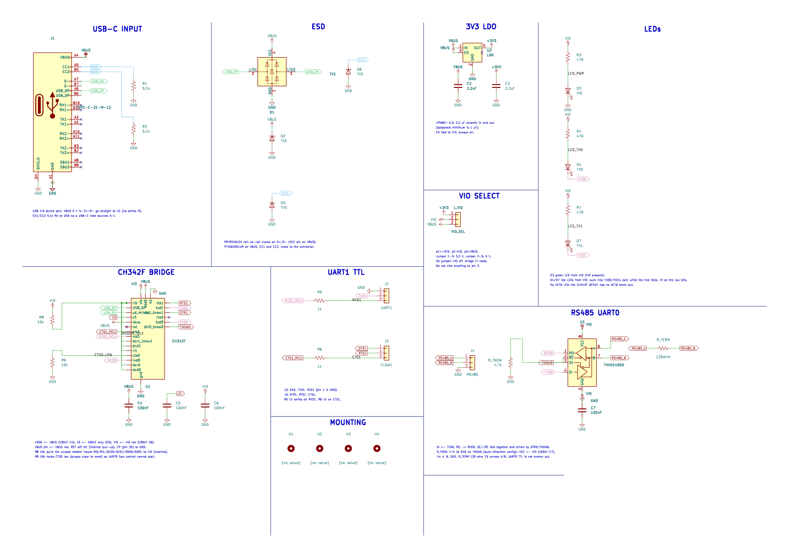
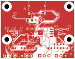
Parts
| Reference | Part | Role |
|---|---|---|
| U1 | WCH CH342F | USB to dual UART bridge |
| U3 | TI THVD1450D | RS-485 transceiver, direction set automatically |
| D1 | Nexperia PRTR5V0U2X | ESD array on the USB data pair |
| D2 D5 D6 | Nexperia PTVS6V0S1UR | TVS diodes on VBUS, CC1 and CC2 |
| R_TERM | 120 Ω resistor | Bus termination, permanently across A and B; there is no jumper |
| U2 | TI LP5907 | 3.3 V low-noise regulator |
| J1 | USB-C receptacle | HRO TYPE-C-31-M-12: power and data in. KiCad's 3D model is not installed, so the viewer shows only its outline |
| H1 to H4 | M2.5 mounting holes | Four 2.5 mm holes, two in the top corners and two at the sides |
| J_VIO | 3-pin jumper | Picks 3.3 V or 5 V for the serial I/O |
| D3 D4 D7 | Lite-On LTST-C190 LEDs | Green on VIO; red TX LEDs on TXD0 and TXD1, fed from VIO, so they are dark while a line idles |
| J2 J3 J4 | 3-pin headers | TTL serial, flow control and the RS-485 bus |
Checks
What was measured, and what was not.
Measured
- Routing
- 26 nets connected, 0 open
- KiCad design-rule check
- 0 errors, 0 warnings, 0 unconnected items, from `kicad-cli pcb drc --severity-all --refill-zones` with the project's custom rules (copper to a board edge 0.3 mm, to a hole or an NPTH hole 0.2 mm, from the JLCPCB profile). The ground pour is one connected cluster. Report: reports/usb_uart.drc.json
- Schematic ERC
- 0 errors, 1 warning (a MODEM_IDLE label on more than one wire of the same net), run with the KiCad libraries installed. Report: reports/usb_uart.erc.json
- Release gate
- Passed: release_ready and fabrication_ready are true in Synth's records. That means Synth's own checks passed (routed, 0 open nets, KiCad DRC clean). It is not a manufacturing sign-off: nothing was fabricated or tested, and the fabrication note below applies. Records: reports/usb_uart.routing.json, reports/release.json
- Fabrication note
- One via-in-pad: the U1 exposed-pad ground via at (23.8, 17.3) mm needs filled and capped vias at the fab. Not confirmed with JLCPCB for this board.
- Copper
- 273 track segments, 43 vias, 515.4 mm. 213 segments on F.Cu and 60 on B.Cu; every via is a through via between the two copper layers.
- Signal integrity
- 23 warnings, none blocking: every one is a layer change with no ground return via within 1.53 mm, so the return current has to jump between the F.Cu and B.Cu pours. None is on the USB pair, which stays on F.Cu with no via. Nobody has judged them.
- Time to route
- 211 s, from the route record. The router is sensitive to placement: J3 at x 27.0 mm and J4 at x 36.1 mm split the ground pour and left DTR1 unrouted, and 0.5 mm shifts left other nets open. Three exports of the committed inputs gave a byte-identical board on one machine; another machine or FreeRouting version was not tried.
- Router
- FreeRouting 2.4.1. Record: reports/usb_uart.routing.json
- Published files
- Board, schematic, source, layout and report files are byte-identical to absmach/synth#103 as merged, commit de3613e (qualification/class-b/usb-uart/). The 3D model, copper-layer SVGs, schematic SVG and the render are made from that board by KiCad 10.0.7 with the ground pours refilled.
- Synth build
- The routing and release reports were produced on Synth e6455e1, the source_revision recorded in reports/release.json.
Not claimed
- Two copper layers and no declared stackup: the exporter writes the 1.6 mm default. There is no inner reference plane, so a return current under an outer-layer track has to use the F.Cu or B.Cu ground pour.
- The USB pair is not impedance-controlled or coupled. A 90 Ω differential pair needs about 1.18 mm traces at 1.6 mm on two layers, so no impedance target is declared. Measured by the author on the committed board: both lines are on F.Cu with no via, 38.63 mm (D+) and 13.52 mm (D-), 25.11 mm of skew (about 0.2 percent of a 12 Mb/s bit), 91.4 percent of the length over solid B.Cu ground fill. Not an independent review.
- The signal-integrity pass reports 23 layer changes with no ground return via within 1.53 mm (V3, LED_TX1, RXD0, +3V3, CTS0_LOW, RXD1, TNOW0, MODEM_IDLE, DTR1 and VBUS). None is on the USB pair. Nobody has judged them.
- FreeRouting's escape analysis flags J1 and U1 (0.5 mm pitch): neither a minimum via nor a minimum track fits between adjacent pads, and it suggests 4 layers. The route completes, with the only via-in-pad at U1 pin 25.
- R_TERM (120 Ω 1 %) is permanently across A and B; the registry part for a 2-pin jumper (header_1x2) is not on this board. Every node on the bus is terminated whether or not it is the end node. Intended use is bench or lab, short cables, point-to-point or the last node on a bus.
- The RS-485 pair has no external TVS and no common-mode choke. Only the THVD1450's on-chip ±18 kV IEC contact ESD protects the bus; TI's 1 kV surge circuit is not built and the bus is not surge-tested. A surge TVS, series resistors and a selectable termination are left for a later revision.
- The U1 exposed-pad via needs filled and capped vias. JLCPCB has not been asked about this via. Its quote flow accepted the previous revision of the board on 2026-10-27 and the Gerbers were regenerated for this one, but the quote, BOM matching and DFM findings were not redone.
- No VBUS bulk capacitor, fuse, or reverse and inrush protection.
- J1 courtyard to the top board edge is 0.01 mm: the shell face sits 0.50 mm inside Edge.Cuts, and the enclosure cutout fit is not checked. The J1 connector datasheet was not read. The Lite-On LED numbers are second-hand. The CH342F exposed pad is 2.6 mm in the KiCad footprint and 2.4 mm in the supplier drawing. Part availability, JLCPCB assembly and the registry LCSC numbers were not checked.
- Header pin labels (GND, TXD1, RXD1 and so on) exist only in the schematic: Synth has no silkscreen text for them. Only the reference labels D7, J4, J_VIO and U1 are placed by hand in the sidecar.
Files
Everything on this page, to open in your own tools.
- Design sourceThe .synth file Synth compiles
usb_uart.synth - Placement layoutWhere each part sits on the board, in board millimetres
usb_uart.placement.layout.toml - KiCad PCBRouted board
kicad/usb_uart.kicad_pcb - KiCad schematicGenerated sheet
kicad/usb_uart.kicad_sch - KiCad symbolsGenerated symbol library
kicad/usb_uart.kicad_sym - KiCad projectProject settings
kicad/usb_uart.kicad_pro - KiCad custom rulesCopper to a board edge 0.3 mm, to a hole or NPTH hole 0.2 mm, from the manufacturer profile
kicad/usb_uart.kicad_dru - Bill of materialsReference, value, description
kicad/bom.csv - 3D modelBinary glTF, as shown in the viewer
usb-uart.glb - 3D model (STEP)The board and component models as a STEP assembly, for CAD and enclosure work. The connector has no installed model, so only its pads appear
usb_uart.step - Route recordSynth's routing run: router, settings, nets, segments, vias
reports/usb_uart.routing.json - Design-rule checkKiCad 10 DRC report for the routed board
reports/usb_uart.drc.json - Schematic ERCKiCad 10.0.7 ERC report for the generated schematic
reports/usb_uart.erc.json - Qualification matrixWhat was checked, what was not, and what is open
QUALIFICATION.md - File hashesSHA-256 of every file in this folder except the zip
SHA256SUMS - Release gate resultSynth's release gate record
reports/release.json - PromptA cleaned version you can run yourself
prompt.md
License
The `.synth` source, layout files, prompt, KiCad project and images on this page are published in the Synth website repository (github.com/absmach/synth-website), which is licensed under Apache-2.0. The Synth compiler that made them is Apache-2.0 too. The LICENSE file in the zip has the full text, including its disclaimer of warranty.
The KiCad project and the 3D model use footprints and component 3D models from KiCad's official libraries. Those libraries are licensed under CC BY-SA 4.0 with an exception: a design that uses them does not have to be shared under that license (see kicad.org/libraries/license). The zip contains this board only, not the libraries.
This is a description of how the files are published, not legal advice. The board is not fabricated and not tested on hardware.